FWDDC for real‑time RF signal processing
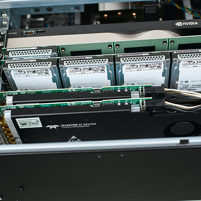 Figure 1. Satellite monitoring system combining two ADQ35 digitizers with FWDDC, SSD storage, and NVIDIA GPU acceleration for high-bandwidth RF signal capture and analysis.
FWDDC is an FPGA-based digital downconversion (DDC) firmware option for frequency-domain applications. It is available for ADQ7DC and ADQ7WB digitizers and is also being evaluated by selected customers as a prototype on certain ADQ3-series models.
Contact us if you are interested in participating in the evaluation program.
The primary purpose of FWDDC is to reduce the digitizer's output data rate, simplifying downstream signal processing and adapting the data stream to a rate that the host PC can handle.
Use case examples:
-
Satellite monitoring and spectrum surveillance (direct RF sampling with digital downconversion of selected bands for baseband analysis)
-
Wideband RF signal capture and channelization (extracting narrowband signals of interest from multi‑GHz bandwidth inputs)
-
Software-defined radio (SDR) and communication systems (real-time downconversion to complex I/Q for demodulation and decoding)
-
Radar and EW signal analysis (frequency translation and decimation to isolate targets or chirps while reducing data throughput)
-
Multi-channel and MIMO systems (synchronized downconversion of multiple RF channels for coherent processing)
-
Automated test and measurement (ATE) (band-selective acquisition and data reduction for faster test cycles and lower storage needs)
-
Real-time spectrum monitoring and interference detection (continuous streaming with FPGA-based downconversion for long-duration captures)
-
Digital receiver prototyping and research (flexible NCO-based frequency tuning and baseband extraction without analog front-end changes)
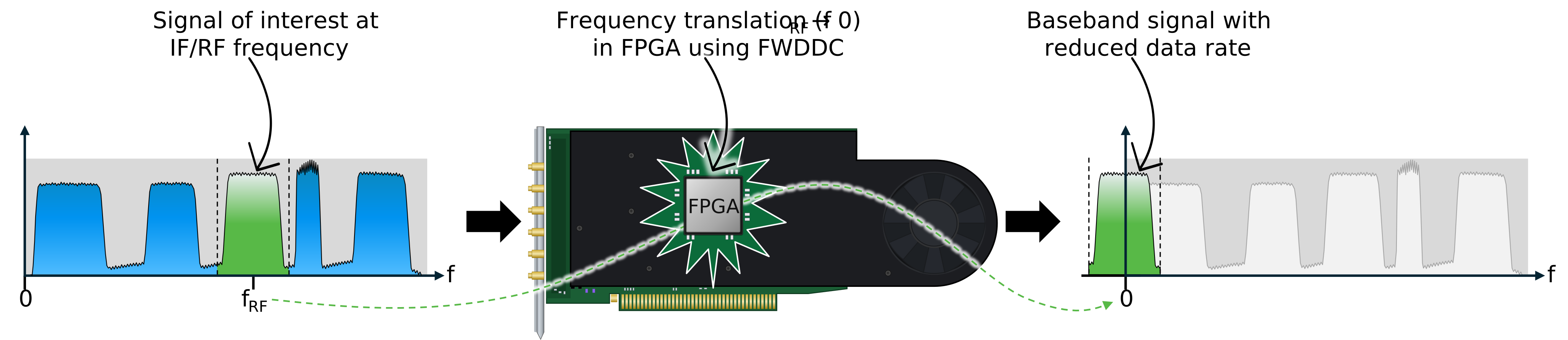 Figure 2. FWDDC digitally extracts a user-defined frequency band from a wideband RF spectrum, translates it to baseband (0 Hz),
and reduces the output data rate through filtering and decimation performed in the onboard FPGA.
Key Benefits of FWDDC
-
Reduce data transfer rates without sacrificing front-end performance
Transfers only the bandwidth of interest while maintaining full ADC sampling speed.
-
Lower CPU, GPU, and storage requirements
FWDDC reduces the amount of data that must be transferred, stored, and processed, enabling more cost-efficient host system architectures.
-
Enable continuous streaming of high-bandwidth RF signals
Helps keep data rates within the limits of interfaces such as PCIe, supporting long-duration acquisitions and continuous real-time streaming.
-
Focus processing resources on the signals that matter
Allowing downstream software and GPUs to concentrate on signals of interest rather than the entire digitized spectrum.
-
Deploy without FPGA development
Utilizes the FPGA already available onboard, eliminating the need for custom FPGA development while reducing integration effort and time-to-market.
-
Scale from single-channel to synchronized multi-board systems
Built-in synchronization support phase-coherent operation across multiple channels and digitizers, making FWDDC suitable for applications such as phased arrays, MIMO systems, and direction finding.
How FWDDC Works
FWDDC performs digital downconversion directly in the FPGA of the digitizer (figure 3). For digitizers that support direct RF sampling across multiple Nyquist bands, an external analog filter is first used to select the frequency band of interest before digitization. A programmable NCO then shifts the selected signal band to complex baseband (I/Q), while decimation filters reduce bandwidth and output data rate before transfer to the host PC. This allows wideband RF signals to be processed efficiently while significantly reducing data throughput.
By transferring only the bandwidth of interest, FWDDC minimizes data throughput while preserving the information required for further signal processing in software running on a CPU or GPU.
Please note that the firmware reduces the data rate to the PC, but it is not a complete RF / IF receiver. Application-specific receiver functions such as channel filters, demodulation, decoding, or direction finding must be performed on a CPU or GPU (figure 3).
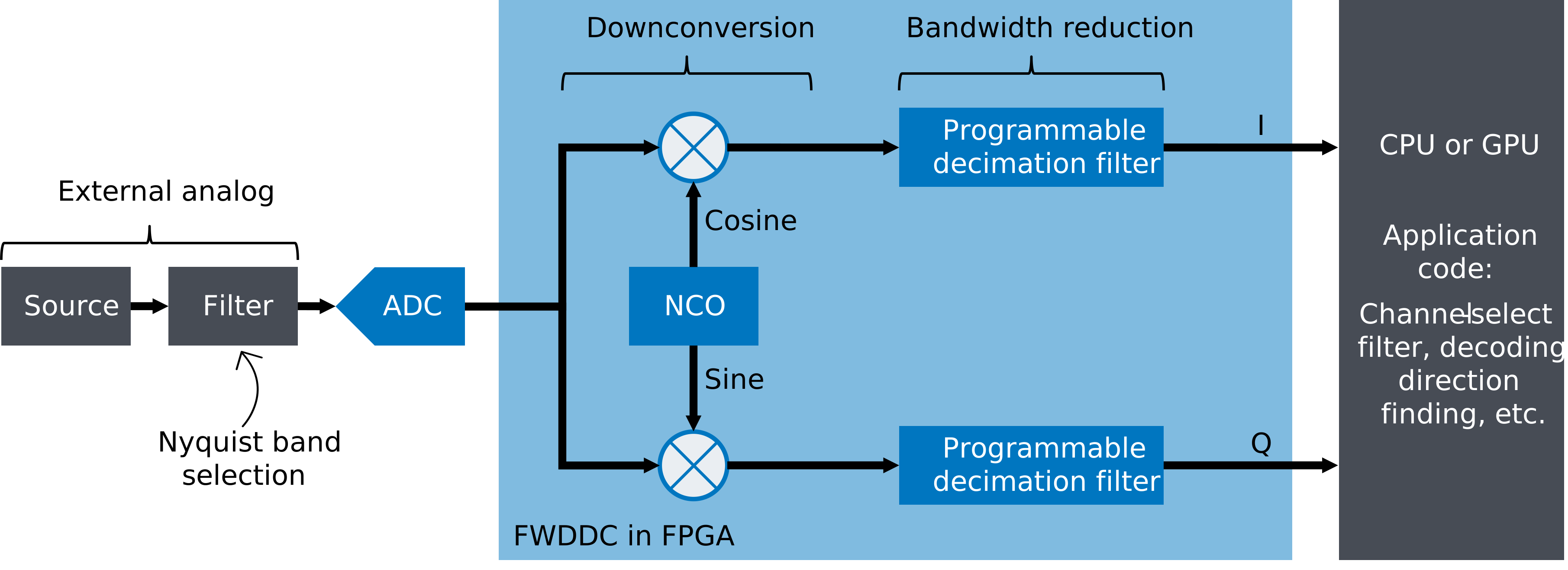 Figure 3. Signal processing chain used by FWDDC to select, downconvert, and stream only the bandwidth of interest to the host computer. One DDC instance is used per digitizer channel.
Supported Hardware and Performance
Model
|
Analog Bandwidth |
FWDDC Channel Modes |
Sampling Rate |
Max bandwidth(1) |
Max Data Transfer Rate |
Availability |
|
ADQ7DC |
3 GHz |
2-ch |
5 GSPS |
2 GHz |
7 Gbyte/s |
Production |
|
ADQ7WB |
6.5 GHz |
2-ch |
4 and 5 GSPS |
2 GHz |
7 Gbyte/s |
Production |
|
ADQ35-WB |
9.0 GHz(2) |
1-ch / 2-ch |
3 to 10 GSPS |
4 / 2 GHz |
14 Gbyte/s |
Evaluation |
|
ADQ35 |
2.5 GHz |
1-ch / 2-ch |
3 to 10 GSPS |
4 / 2 GHz |
14 Gbyte/s |
Evaluation |
|
ADQ36 |
2.5 GHz |
4-ch |
2.5 GSPS |
1 GHz |
7 Gbyte/s |
Evaluation |
|
ADQ32 |
2.5 GHz |
1-ch / 2-ch |
2.5 and 5 GSPS |
2 / 1 GHz |
7 Gbyte/s |
Evaluation |
(1) Supported instantaneous bandwidth is 80% of the selected Nyquist band.
(2) Useable analog bandwidth at -6 dB.
Example Frequency Coverage for ADQ7WB
Many digitizers support direct RF sampling across multiple Nyquist bands. The band of interest is selected using an external analog filter, while the digitizer sampling rate and analog input bandwidth determine which frequency ranges can be acquired. Models supporting multiple sampling rates provide additional flexibility when planning frequency coverage. Figure 4 shows example frequency coverage for ADQ7WB operating at 5 GSPS (top) and 4 GSPS (bottom). Supported bandwidth within each Nyquist band scales with sampling rate, while coverage in the highest Nyquist band is ultimately limited by the digitizer's 6.5 GHz analog input bandwidth.
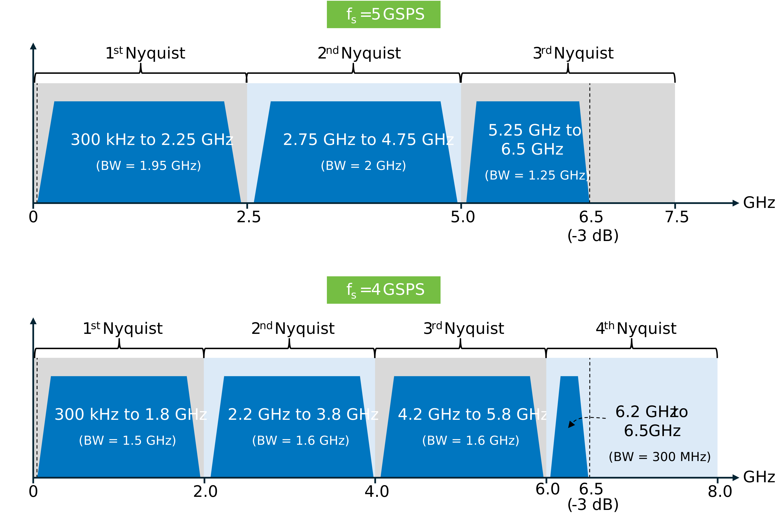 Figure 4. Example frequency coverage for the ADQ7WB digitizer at 5 GSPS (top) and 4 GSPS (bottom). The supported frequency bands differ between sampling rates and are determined by the Nyquist zones and the digitizer's analog input bandwidth.
Frequency Planning Example using ADQ35-WB
ADQ35-WB supports direct RF sampling across multiple Nyquist zones and offers several sampling-rate options in both single-channel and dual-channel modes. The figure below illustrates example frequency coverage for common L-, S-, and C-band signals and highlights how sampling rate and operating mode affect the available FWDDC bandwidth.
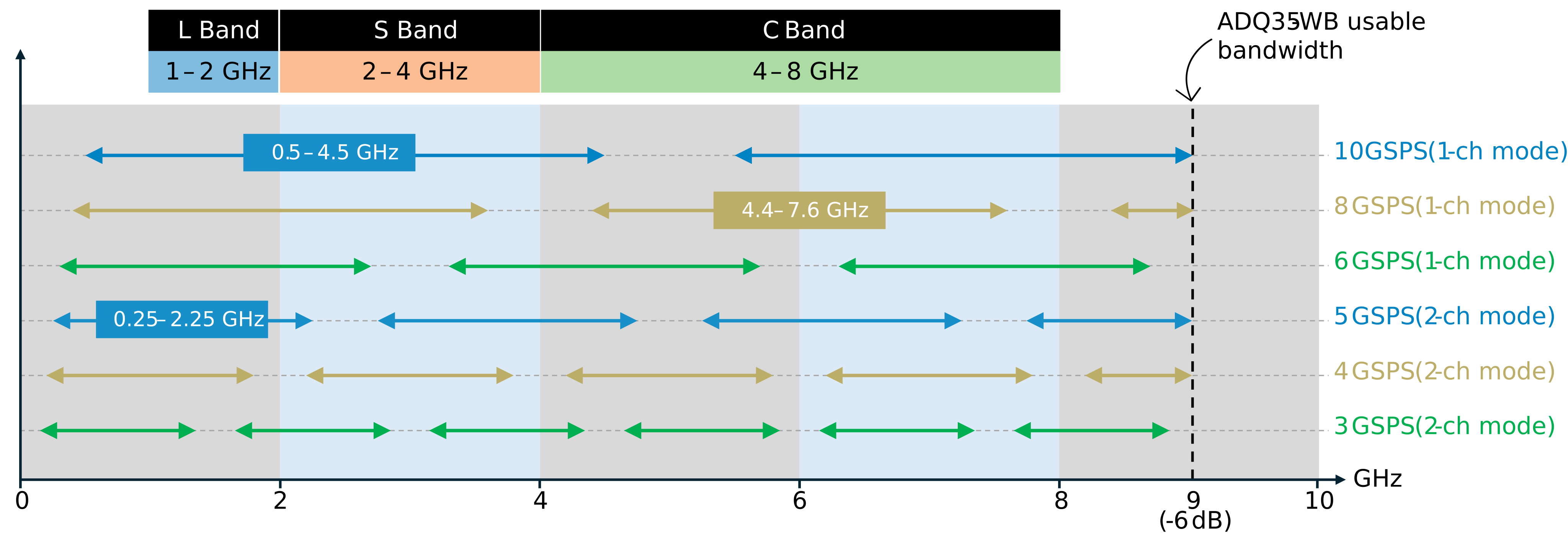 Figure 5. Frequency planning example illustrating direct RF sampling of L-, S-, and C-band signals with ADQ35-WB.
Highlighted examples shown in Figure 5:
- Full S-band coverage using ADQ35-WB in single-channel mode at 10 GSPS sampling rate (supporting 0.5 to 4.5 GHz band)
- Extensive C-band coverage using single-channel mode at 8 GSPS
- Entire L-band coverage at 5 GSPS in dual-channel mode
- Dual-channel operation enables simultaneous acquisition on two channels while still providing wide frequency coverage across multiple Nyquist zones
Two-tone Downconversion Example
The figure below illustrate a two-tone test demonstrating digital downconversion and decimation using FWDDC on an ADQ35-WB sampling at 5 GSPS. Narrowband signals at 2790 MHz and 2810 MHz are translated to baseband using an NCO tuned to -2800 MHz, followed by decimation from 1× (no decimation) to 64×.
Figure 6. The animation shows the effect of increasing decimation after digital downconversion.

