Webinar

We explain how high-performance digitizers combined with real-time digital signal processing...

View Webinar →
 

Webinar

Digitizer with integrated dual-gain amplifier for maximizing dynamic range in pulse measurements

View Webinar →
 

Video

Introduction of data acquistion solutions for Time-of Flight Mass Spectrometry Solutions

View Video →
 

Video

A brief 2-minute introductional video of our technology Pulse Dynamic Range Extension (PDRX)

View Video → ​​​​​​​​​​​​​​​​​​​​​​​​​​​​​​​

Time-of-flight mass spectrometry (TOFMS) is an analytical technique that separates ions based on their mass-to-charge ratio (m/z) by measuring the time required for ions to travel through a field-free flight tube. After acceleration by an electric field, ions are separated according to their velocities — lighter ions reach the detector before heavier ones.

The digitizer plays a critical role in TOFMS systems by capturing the transient electrical pulses generated when ions strike the detector. These pulses are typically very brief (nanoseconds to microseconds) and must be sampled at high rates with sufficient resolution to accurately quantify ion abundance across a wide dynamic range.

​​Modern TOFMS applications demand digitizers capable of not only high-speed acquisition but also advanced signal processing, baseline stabilization, and data reduction to handle the enormous data volumes generated during high-throughput analysis. The basic principle is illustrated in figure 1.​

Figure 1. Basic functional elements of a time-of-flight mass spectrometry system.​

  • 1. Ions that hit the detector generate short-lived pulses - often in the range of 500 - 700 picoseconds (full width at half maximum, FWHM).
  • 2. The total flight time often needs to be recorded and typically vary from 10 µs to 100 µs.
  • 3. Acquired pulses are unipolar and mostly negative-only (negative polarity).
  • 4. Pulse acquisition is commonly done using a level trigger, where the trigger level is set relative to a baseline (DC level).
  • 5. The detector's output often contains a combination of strong and weak signals due to difference in ion concentration within the sample substance.
  • 6. Ions with similar m/z will hit the detector almost at the same time, and it is important to be able to distinguish them.
  • 7. The acquired signal may contain either dense or spare pulses, depending on the ion concentration.
  • 8. The digitizer need to fit within the confined space of the MS system and should be located close to the detector so that short cables helps minimize signal reflections.
  • 9. It is beneficial to use digitizers with hardware trigger output so that they can trigger the ion source with accurate timing.

DC Offset Adjustment

Programmable DC offset allows users to maximize the effective input range while preventing signal saturation. This feature is critical in TOFMS where baseline drift can cause signals to shift outside the optimal digitizer range.​​


Figure 2. DC offset is a crucial feature needed to fully utilize the digitizers input range while avoiding overflow/saturation.​

Digital Baseline Stabilizer (DBS)

Corrects slow baseline drift caused by temperature variations, detector aging, or environmental factors. The DBS continuously monitors and compensates for DC shifts, ensuring stable measurements throughout extended acquisition sessions.


Figure 3. Uncorrected baseline fluctuation/drift may result in missed pulses (top). With DBS this is corrected (bottom).​

FPGA-Based Data Reduction

On-board FPGA processing enables real-time peak detection, integration, and data compression. This significantly reduces the volume of data transferred to the host system while preserving critical signal fidelity and measurement accuracy.​


Figure 4. The onboard FPGA is crucial for reducing the data rate so that it matches t​he link capacity without loss of signal information.​

Precise triggering when using accumulation

Averaging involves accumulating a large number of waveforms (records) and subsequently scaling by the total number of accumulated waveforms. The accumulation functionality is available through the FWATD firmware option. This process effectively suppresses random noise and enhances systematic (periodic) signals.

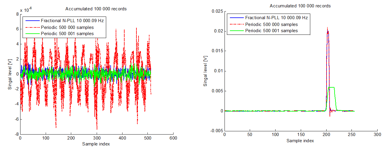
However, when a large number of records are accumulated, systematic noise may become apparent. Refer to the figure below, where the left-hand red curve illustrates accumulated systematic noise at 6 µV. This type of noise is amplified when the trigger is correlated with the noise source.

To mitigate this, decorrelating the trigger frequency from the noise source can suppress the systematic noise. The green and blue curves in the figure demonstrate the resulting noise suppression.

Decorrelation can be achieved through various methods, though care must be taken to avoid introducing jitter. In the right-hand figure, the green pulse exhibits jitter and is broadened as a result. In contrast, the red and blue pulses remain sharp, indicating the absence of jitter.

The ADQ35 and ADQ35-PDRX digitizers incorporate a fractional-N PLL-based trigger source, which enables both systematic noise suppression and low jitter performance, as demonstrated by the blue curves in both plots.

For further details, refer to the application note 25-3162 ADQ35-PDRX FWATD trigger 


The application note outlines a method for achieving noise suppression during waveform accumulation. It is recommended for use with the ADQ35 and ADQ35-PDRX devices when accumulating a large number of waveforms.

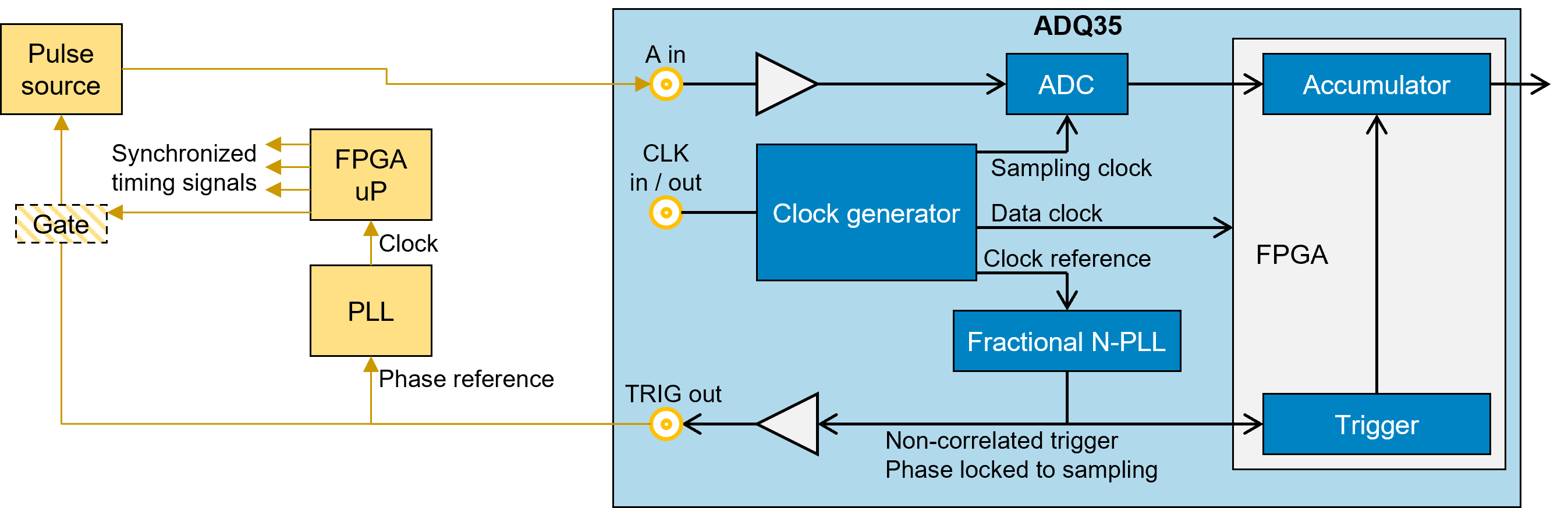
The method relies on a Fractional-N PLL, which requires the ADQ35 to act as the timing master within the system. This may necessitate some system-level redesign. For scenarios where only the pulse source needs to be triggered, figure 7 in the application note provides a viable solution. If more precisely controlled signals are required, this approach remains applicable but with minor modifications.

In this configuration, the Fractional-N PLL triggers the pulse source and simultaneously serves as a clock reference for an FPGA or microprocessor, the generation of states and control signals as illustrated below.

If the trigger rate is too low to support PLL operation, a higher frequency can be used, with a gating mechanism applied to set the desired trigger rate for the pulse source.

This setup ensures synchronization across all system components, enhancing timing precision and signal integrity.


Teledyne SP Devices offer both stand-alone firmware packages as well as firmware development kits:

  • FWATD is an optional stand-alone firmware package that provide extreme dynamic range through noise reduction. It provides four methods for noise reduction; DBS for stable trigger reference (baseline​) level, low-pass filter for noise suppression, threshold for detection of rare events, and real-time waveform averaging of repetitive signals for power enhancement. This firmware is commonly used in mass spectrometry and have in some instances helped reduce the output rate from 20 Gbyte/s to 40 Mbyte/s - a reduction of 500 times without loss of signal properties/characteristics!
  • FWPD provides pulse detection capabilities including tools for detecting sparse, non-repetitive pulses. It outputs either pulse metadata, raw pulse data captured within a detection window, or both. It also discards unwanted data in order to reduce the overall data rate. In mass spectrometry this firmware is used for determining peak location, pulse width, etc.
  • The ADQ Development Kit is a tool for developing custom digitizer firmware. In mass spectrometry it can for example be used to implement real-time curve fitting to distinguish pulses that overlap.
  • In some MS systems it is desirable to either post-process the data in graphics processing units (GPUs) or record data to disk storage. In both cases it is beneficial to use peer-to-peer (P2P) technology that enables direct data transfers between the digitizer and GPU or storage. This is a huge advantage compared to conventional solutions that put a lot of stress on both the CPU and RAM of the host PC. With P2P, both the CPU and RAM can instead be used for other tasks. Learn more about peer-to-peer here.
  • With LICPDRX, customers gain access to the DSP blocks utilized in PDRX. By utilizing two 12-bit analog-to-digital converters we have achieved a dynamic range equivalent to commercial 16-bit converters. This optional paid license enables PDRX as an add-on to existing firmware options (FWDAQ, FWPD, etc.) for selected dual-channel digitizers.

Want to learn more about the technical details and advantages? Download our white paper below! ​​​​​​​


FWATD

Optional stand-alone firmware package that provide extreme dynamic range through noise reduction.

Explore →
 

FWPD

Provides pulse detection capabilities including tools for detecting sparse, non-repetitive pulses.

Explore →
 

ADQ Development Kit

Enables customized real-time signal processing and can help reduce the total amount of data transferred to the host PC. ​​

Explore → ​
Image Model Resolution Channels Sampling Rate Coupling Input Bandwidth ENOB max Interface
ADQ35 ADQ35 12-bit 1
2
10 GSPS
5 GSPS
DC 2.5 GHz 8.4 bits PCIe, USB 3.2
ADQ7DC ADQ7DC 14-bit 1
2
10 GSPS
5 GSPS
DC 3 GHz 9.1 bits PCIe, PXIe, USB 3.0, MTCA.4, 10GbE
ADQ14 ADQ14 14-bit 1
2
4
2 GSPS
2 GSPS
1 GSPS
DC, AC 1.2 GHz 10.2 bits PCIe, PXIe, USB 3.0, MTCA.4
ADQ35-PDRX ADQ35-PDRX 12-bit 2 5 GSPS DC 2 GHz 11.0 bits PCIe
ADQ32-PDRX ADQ32-PDRX 12-bit 1 2.5 GSPS DC 760 MHz 11.6 bits PCIe, USB 3.2
ADQ32 ADQ32 12-bit 1
2
5 GSPS
2.5 GSPS
DC 2.5 GHz 9.2 bits PCIe, USB 3.2
ADQ33 ADQ33 12-bit 2 1 GSPS DC 760 MHz 9.4 bits PCIe, USB 3.2
ADQ33-PDRX ADQ33-PDRX 12-bit 1 1 GSPS DC 1 GHz 11.5 bits PCIe, USB 3.2

Firmware options​​​​​​ C​omment​​​​
FWATD​ Optional w​aveform averaging firmware. ​
FWPD​ Optional pulse detection firmware.​​​​​​​​​​​​​​​​​​​​​​​​​​​​ ​​​
DEVDAQ​ Optional FPGA development kit based​​ on FWDAQ. ​